- Building Machines In Code
- Building Machines in Code – Part 2
- Building Machines In Code – Part 3
- Building Machines In Code – Part 4
- Building Machines In Code – Part 5
- Building Machines In Code – Part 6
- Building Machines In Code – Part 7
- Building Machines In Code – Part 8
- Building Machines In Code – Part 9
Post Stastics
- This post has 2141 words.
- Estimated read time is 10.20 minute(s).
What is a CPU and How Does it Work?
Today, we will continue to learn about emulators and simulators. I know last time I left you with only words and many of you just can’t wait to get to the code! Patience Grasshopper, good things come to those who wait… Today our mission is to simply cover some basic computer and CPU architecture. I promise after a short read today, we’ll have enough foundation to begin to build our machines in code.
What is a CPU?
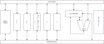
A CPU or Central Processing Unit is the portion of the computer around which all other systems are built. It is often referred to as the brains of a computer system. The CPU performs arithmetic and logical operations. Most CPUs consist of an ALU (Arithmetic Logic Unit) for performing calculations and logic operations, a CU (Control Unit) which manages the various components of the CPU, a Register Store for holding the values to be worked on, and various BUSs for transferring data in and out of the CPU. These can include a memory address bus, control bus, data bus, and an I/O (input/output) bus.
Internally, the CPU contains various registers. A register is like a small storage location. A CPU may have a single register or many registers. For example, the MOS 6502 processor contains 6 addressable registers. These include the Accumulator, X, and Y index register, a Program Counter (PC) register, a Stack Pointer (SP) register, and a Processor Status (P) register.
The Accumulator or “A Register” is used to both provide data to the ALU and hold the results of the ALU operations. Additional data can also come from memory. For example, when doing addition one operand will be provided in the A register while another will be provided from memory.
Most processors have more registers than the 6502. For example, the Motorola 6800 CPU contains two accumulators, A and B. Both of these registers can provide data to the ALU and accept results from the ALU when performing operations. Many modern CPUs have dozens of registers. Some are for special purposes and can only be used for certain types of operations while others are for more general use.
The Instruction Cycle
All CPUs at their core do the same basic operations. Just as there are many makes, models, shapes, and sizes of automobiles, there are many makes, models, shapes, and sizes of microprocessors. Some are built for performance, some for ease of use, and some for special purposes. Their prices range from a few cents (see the PMS150C a 3¢ cent processor at LSCS Electronics) to $60k for some high-end server processors, to hundreds of thousands of dollars for some custom supercomputer processors. But at their core, they all follow the same three basic steps: Fetch, Decode, and Execute.
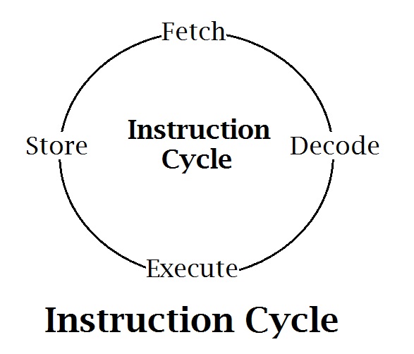
When power is first applied to a CPU the processor goes through an initialization cycle. This is often referred to as the reset cycle since it is often controlled by a reset signal. The purpose of this cycle is to place the processor in a known state from which to begin program execution.
Next, the processor must fetch an instruction from program memory and then decode it to learn what operation it needs to perform. These are the Fetch and Decode cycles. With the instruction decoded, the processor then executes the instruction. These three steps are performed over and over by all typical computer processors.
CPU Archietypes: CISC vs. RISC
CISC (pronounced “Sisk”) or Complex Instruction Set Computers are microprocessors that contain many (sometimes several thousand) instructions. They follow a design philosophy of “providing instructions for complex operations”. This was good when these processors only had 30 – 50 instructions. But now, they often have thousands of instructions. Try remembering all those instructions! With so many to choose from, it is often hard to find the right instruction. Often there are multiple instructions capable of producing the same results but one will be more efficient in certain circumstances than the others. CISC processor instruction often takes many CPU cycles to complete. While this may make them appear slow compared to RISC processors, the “complex” instruction they contain do more work per cycle than those of a RISC processor.
RISC or Reduced Instruction Set Computer processors have simpler instructions than their CISC counterparts. They often complete one instruction per CPU clock cycle, and some can even complete multiple instructions per CPU clock cycle for certain instructions. RISC instructions are much simpler and perform basic operations. This makes them fast! However, they are doing less work per cycle than their CISC cousins.
Today’s modern processors have evolved to include elements of both processor archetypes. The Intel 80xxx series (x86) used in most modern computers are CISC processors. But the industry has introduced a new standardized ISA (Instruction Set Architecture) processor to be phased in over the next few years that is a RISC V (Pronounced – Risk Five) architecture. The ARM processors found in most mobile phones and many tablets are also RISC processor designs. In fact, the ‘R’ in ARM (Acorn RISC Machine) stands for RISC.
So which is better? The answer to this question, like so many things in computer science is “it depends”. As stated earlier CISC processors have instructions that do more work per clock cycle so the programmer doesn’t need to write as much code and can sometimes think about their code at a slightly higher level than the RISC programmer. That said, often RISC programmers can coax performance out of their applications, which is difficult to achieve with a CISC processor due to the higher granularity of the available instructions on a RISC processor. Also, RISC processors are typically more power efficient due to their relative simplicity, so they are often chosen for power-critical applications such as mobile devices.
Fixed vs. Stored Program Computers
Early computers did not hold their programs in RAM (Random Access Memory). Instead, they stored their programs in ROM (Read Only Memory). The early ROMs were programmed during manufacturing. A programmer would write the program and send it off to be placed in a ROM chip. It often took months to receive a new ROM back from the manufacturer. When the ROM arrived it often contained flaws in the program. The only way to correct these flaws was to rewrite the program and again send it off to the ROM manufacturer and wait another couple of months. It could take a year or more to get a program right! These early computers could not change their programming. They ran one program and no other.
These machines were known as “Fixed Program” computers because their program was permanently fixed into the machine. Because of this, these machines booted almost instantly. They required less RAM because the program wasn’t loaded into RAM before executing it and they never lost their programming from power outages. They could lose data during power outages but, not programming. Today there are very few examples of Fixed Program computers. There is one common product however that is still a Fixed Program machine and that is the cheap dollar store calculator!
The major drawback to Fixed Program computers was that you could not change the programming. You can’t take that dollar store calculator and run a word processor on it. It’s a calculator and that is all it will ever be. You can’t update its programming to give you new functions. It will remain as it was the day you purchased it. This meant if you needed a calculator and a word processor you had to have two completely different systems.
To solve this issue Stored-Program computers were invented. With a Stored Program computer the program is stored on a storage device such as a disk drive, magnetic tape, or solid-state disk. When the computer is powered up it loads the program from the storage device into the computer’s RAM. Once loaded the program is executed. Because the program is not permanently fixed in the computer, it can be updated or swapped for another program. This is how modern computers are capable of running many different programs. In these machines, a small ROM holds a small boot loader (a tiny program used to load another program from the storage device into the computer’s RAM) that runs when the computer first powers up. All modern computers are designed as Stored Program computers.
Architectures: Harvard vs. Von Neumann
Most computer systems today follow one of two typical system architectures or some combination of them. In a Harvard architecture, the system is configured to have separate program and data memory. This architecture is popular with micro-controllers and gives the system security against the program being modified at run-time. In most systems with a Harvard architecture, the program memory is read-only or requires some special access level to modify its contents.
John Von Neumann thought that programs should be treated as just more data. That is, they should be modifiable at run-time and relocatable in memory even if some special handling is required to do so. The Von Neumann architecture is used in all modern PCs today. In this architecture, the memory does not distinguish between programs or data. It is possible in these machines to write a program that can modify itself in memory as it runs. This has huge security issues, however, and modern CPUs have had features added to segregate memory so that each application can only access the memory it has been allotted.
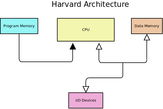
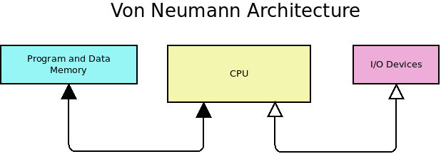
One sector of micro-computers still uses Harvard Architecture today. That is the Micro-controller market. Many small, inexpensive micro-controllers still separate their program code from their data memory. This has the advantage of making the code more secure and the system less complex.
You may think that adding program memory would make the system more complex. However, having the program stored in a separate Read-Only Memory (ROM) reduces the complexity of dealing with instruction fetching and memory operations.
I/O: To Map or Not to Map
I snuck a small detail into the CPU architecture diagrams above. You probably didn’t notice the different arrangements of the I/O devices. A CPU designer has two basic options when it comes to designing access to the I/O devices. They can provide a special I/O space in the CPU, accessing it using I/O instructions, or they can use part of the memory address space for I/O and use standard memory access instructions to operate on I/O. The latter is known as “Memory Mapped I/O”.
Endianness
Endianness refers to the way values are stored in the computer’s memory and registers. Multi-byte and multi-word values can be stored or transmitted in one of two ways. Let’s take a 16-bit value on an 8-bit system as an example. A 16-bit value will require two 8-bit bytes to contain it. This 16-bit value must be split into two 8-bit values typically known as the MSB and LSB. The MSB is the Most Significant Byte and the LSB is the Least Significant Byte.
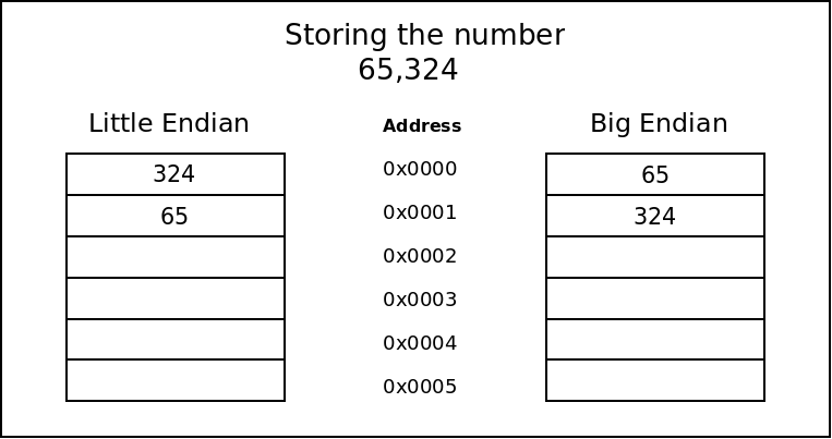
As a system designer, you have two choices for storing this 16-bit value. You can store the MSB first, in the lower address, and then store the LSB in the next (higher) address location (Big Endian) or you could store the LSB in the lower address and the MSB in the higher address (Little Endian).
Another example: Say we want to store the value 769,324 in a system that can only store 3 digits per memory cell. If we store 769 in the lower address and 324 in the following memory address, then the system is Big-Endian. If however, we store 324 in the first address, and 769 in the next address, the system is Little-Endian.
As a simple rule of thumb is to remember which comes first in the address space. If the MSB (big-end of the value) comes first as you walk up the address space, then it is Big Endian. If the small end of the number comes first, then it is Little Endian.
When chip designers design microprocessors they settle on an endianness for their processor. When emulating a system it is important to pay attention to the endianness and implement it correctly.
Conclusion
In this chapter, we have introduced (at a very high level) what a computer is and how they work, and have touched on computer architecture, the instruction cycle, and byte order (endianness). We discussed different computer architectures and fixed and stored program computers. We have a lot to cover and we will revisit most of these topics in later chapters with more detail.
In our next installment, we will finally program a simple Harvard Architecture-based system and work with it a bit.